PCB designs
Introduction
In the rapidly evolving world of electronics, sustainability has emerged as a focal point of innovation.
Electronic circuits, made up of conductive metals, require an insulating and cooling foundation known as a substrate. For the majority of computer chips, this foundation is crafted from non-recyclable plastic polymers. When these chips reach the end of their lifespan, they are typically discarded, adding to the annual 50 million tonnes of e-waste generated. As the environmental impact of electronic waste becomes increasingly evident, scientists like Doris Danninger, Roland Pruckner. Laura Holzinger. Robert Koeppe, Martin Kaltenbrunne are exploring novel materials and methods to address this challenge.
Doris Danninger & his colleagues presents a groundbreaking approach in using & introducing the use of fungal mycelium skins (Mushroom) as a potential substrate for electronic devices.
What is Fungal Mycelium ?
Fungal mycelium is the vegetative part of a fungus, consisting of a mass of branching, thread-like structures called hyphae. These hyphae grow and spread out, forming a network that can penetrate various substrates, such as soil, wood, or other organic materials. This network of hyphae is responsible for nutrient absorption and growth of the fungus.
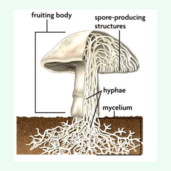 Image Source: Nebraska Statewide Arboretum
When we refer to "fungal mycelium skin," we are talking about a layer or sheet derived from the mycelium. Here's a breakdown:
-
Structure: The mycelium forms a dense, interconnected web of hyphae. When cultivated under specific conditions, this web can create a mat-like structure that resembles a sheet or "skin."
-
Properties: Mycelium skin can be cultivated to have various properties, such as flexibility, strength, and even some degree of water resistance. Its texture can be somewhat similar to leather or felt, depending on the cultivation process.
-
Applications: Due to its unique properties and biodegradability, mycelium skin has been explored for various applications. These include sustainable alternatives to leather, packaging materials, building materials, and, as mentioned in the article, even as substrates for electronics.
-
Sustainability: One of the most significant advantages of mycelium-based materials is their sustainability. They are grown from organic matter, use less water and resources compared to traditional materials, and are biodegradable.
-
Cultivation: Mycelium skin can be grown in controlled environments, where factors like temperature, humidity, and substrate can be adjusted to produce materials with desired characteristics.
Summary of Research:
The research article delves deep into the innovative use of fungal mycelium skins as a potential substrate for the next generation of electronic devices. As the world grapples with the mounting challenge of electronic waste and its environmental repercussions, the need for sustainable solutions in the electronics sector has never been more pressing. The researchers have not only identified but also successfully demonstrated a pioneering method to cultivate and process fungal mycelium skins suitable for electronic applications.
The mycelium skins are versatile and compatible with standard electronic processing methods, such as physical vapor deposition and laser patterning. These techniques enable the creation of electronic traces on the skins, achieving impressive conductivity levels of up to 9.75 ± 1.44 × 10⁴ S cm−1. They are also flexible, enduring over 2000 bending cycles, and maintain functionality even when folded multiple times. The research also showcases high-capacity mycelium batteries that can power devices like Bluetooth modules and various sensors (power upto as high as ~3.8 mAh cm−2) .
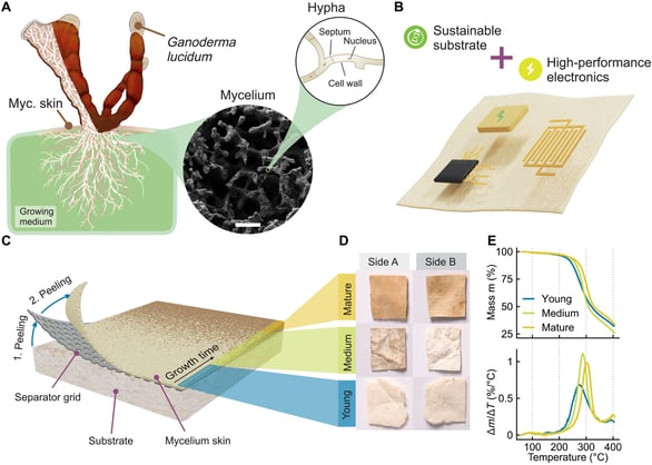
Image source: Science Advance Research Article
(A) Structure of G. lucidum fungus. Mycelium roots are growing inside the chosen medium, with fruiting bodies forming on the surface at longer growth times. Mycelium strains consist of hyphen structures on a microscopic level. Scale, bar 10 μm. (B) Concept of using mycelium skin as substrate for electronic devices. (C) Growth of mycelium skin on PE-separator grid and underlying substrate. (D) Three distinct types of mycelium skin are obtained depending on the growth time. Sides A and B refer to the surface in contact with the surrounding air and the separation grid, respectively. (E) TGA of all mycelium types with a constant temperature change of 0.166 K/s, revealing thermal stability to more than 250°C.
Furthermore, the research doesn't stop at just the substrate. The team ventured into the realm of power sources and showcased mycelium batteries. These batteries boast impressive capacities and have been tested to power a range of devices, from Bluetooth modules to intricate sensors.
For Experts & curious minds who want to dive deep into the reaseach here's the link for the pdf the format: MycelioTronics: Fungal mycelium skin for sustainable electronics.
Thought-Provoking Questions:
- How might the integration of biodegradable materials like mycelium redefine the lifecycle of electronic products?
- Could the adaptability and resilience of mycelium skins lead to new forms of wearable or implantable electronics?
- What are the potential economic implications of transitioning to mycelium-based electronics, considering both production costs and waste management savings?
- How might industries outside of electronics benefit from the properties of fungal mycelium?
Conclusion
The exploration of fungal mycelium skins as a substrate for electronics signifies a promising step towards a greener and more sustainable future in the electronics industry. While the initial results are indeed groundbreaking, the real challenge lies in the scalability and consistent quality of these mycelium-based components in real-world applications. As the world moves towards more eco-friendly solutions, innovations like these not only pave the way for sustainable electronics but also reduce the environmental burden of electronic waste.
Source of article: https://www.science.org/doi/10.1126/sciadv.add7118