
PCB designs

About Author:
Daniel Bogaerts, a distinguished electromechanical engineer who graduated from the Free University of Brussels, spearheaded R&D innovations at Philips where he spent a few years developing switch mode power supplies and advanced particle accelerator development at Ion Beam Applications. Now, as of 2022, he's a sought-after consultant in switchmode power converters and all related aspects, including control and EMC.
Point-of-Load switching converters are nowadays ubiquitous on PCBs, as various supply voltages are often required by different parts of the circuitry while the board itself is generally powered by a unique source. Compared to linear regulators, switching PoLs provide indeed higher efficiency and can step-up the voltages. Being switchers, these converters intrinsically generate sharp current and voltage slopes, emitting broadband noise which may affect the board functional performance as well as its compliance to the EMC standards. Better understanding the noise emission mechanisms leads to simple although sometimes counter-intuitive layout design rules that can greatly reduce the EMC issues of switching PoLs.
This article goes through the principles of PoLs converters and introduces the aspects that make them stop being ideal and the impact on Electromagnetic Compatibility (EMC). A set of rules or design good practices are introduced.
Table of Content:
1. The Canonical Buck Converter
2. Ground connection is inductive
3. Diodes are capacitive
4. The Cure
5. A multilayer PCB is also a current transformer
6. An inductor is also a capacitor
7. Conclusion
1. The Canonical Buck Converter
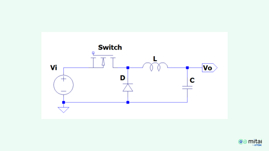
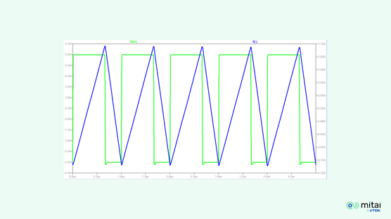
Traditionally, a buck converter is represented as shown below; the diagram is neat and its operation is easy to explain:
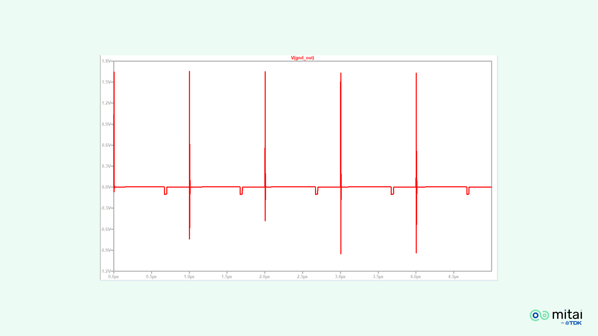
- When the switch is ON, the diode is reversed biased and is thus OFF, the inductor sees the (positive) difference between input and output voltage and the current rises in the inductor according to dI/dt = (Vi - Vo) / (neglecting any voltage drop across the switch).
- When the switch is OFF, the inductor current freewheels through the diode and decreases according to dI/dt = - Vo/L (neglecting the voltage drop across the diode)
In steady state, the average output voltage Vo = Vi . ton / T where ton is the ON time of the switch and T the cycle period, regardless of the output current (provided it is high enough to never drop to zero during the OFF time of the switch). The output capacitor filters out the current ripple in the inductor to provide a continuous voltage on the output.
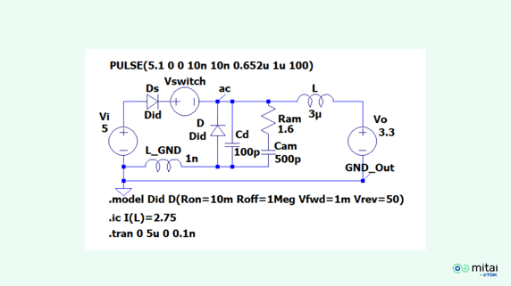
For simulation purposes, we’ll first transform a little bit the schematics:
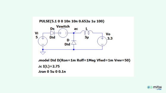
In our example, the buck converter is stepping the voltage down from a 5 V source to 3.3 V.
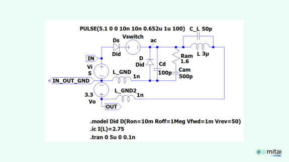
The switch is replaced by a pulsed voltage source (Vswitch) in series with the quasi-ideal diode Ds; when the source voltage is zero, the switch is ON; when the source voltage is 5V, it blocks the diode and the switch is OFF. This is a simple way to pilot the switch while controlling its rate of voltage change; this mimics the behavior of a physical MOSFET transistor, whose dV/dt is limited by the Miller effect.
We make here the hypothesis of a high switching frequency (1 MHz) with transition times equal to 1 % of the cycle period (10 ns). We also suppose that the output capacitor is perfect and infinite, so we can replace it by the voltage source Vo.
Finally, using the initial condition “.ic” directive, we make the converter operate at an output current around 3 A.
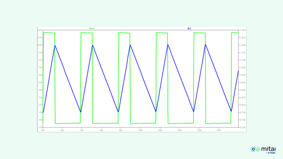
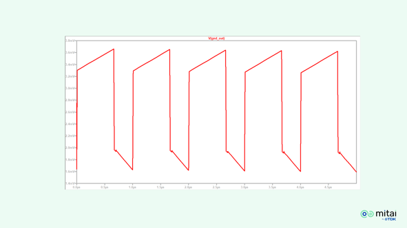
Launching the simulation, we can check that we get the expected near-perfect behavior, with the current in the inductor rising when the input voltage is applied, and decreasing during the freewheeling phase:
2. Ground connection is inductive
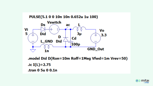
Simulations are nice, but always neglect some part the real life. Let’s consider the ground connection between the input voltage source Vi (in practice, the input capacitor) and the freewheeling diode D. It will most often be implemented by a ground plane in an inner layer, but even so some impedance will be present. Let’s introduce the very small value of 1 nH in this link, i.e. the order of magnitude of the inductance of a 1 mm long wire:
Let's launch the simulation:
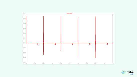
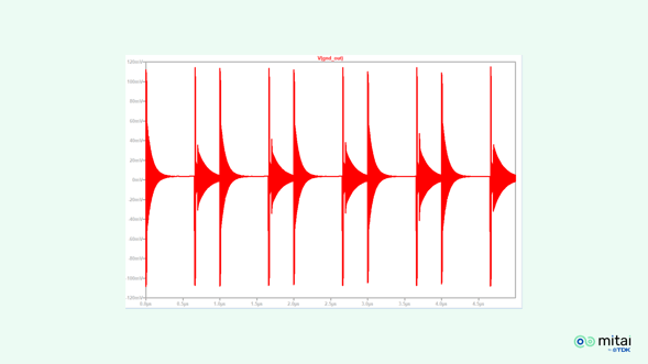
The waveforms are almost unchanged, which is no surprise after all, as 1 nH is a very small value; but let’s have a look at the voltage difference between the input and output grounds (in practice, the negative side of the input and output capacitors):
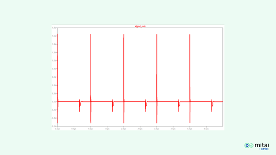
Something is going on there; let’s zoom:
3. Diodes are capacitive
There are very fast oscillations, with a period half the minimum step size specified in the .tran simulation directive (0.1 ns); we are probably missing something. Let’s see if we can get closer to reality by adding another “parasitic” component to the circuit. One obvious candidate is the parasitic capacitance of the diode, as it can come into action precisely at that moment (it was previously shorted by the diode conducting):

The shape of the signal has changed but its amplitude has not decreased.
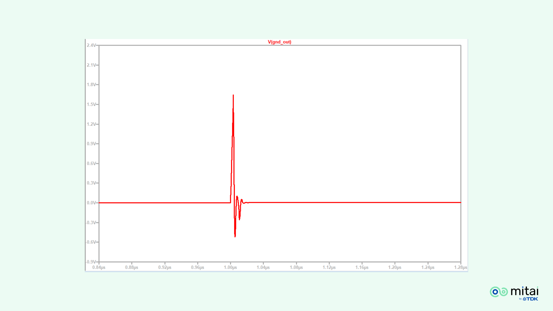
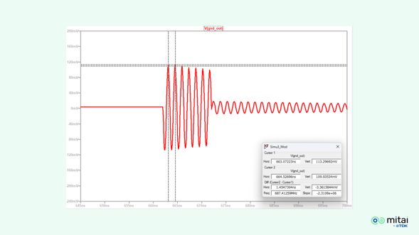
Zooming again:
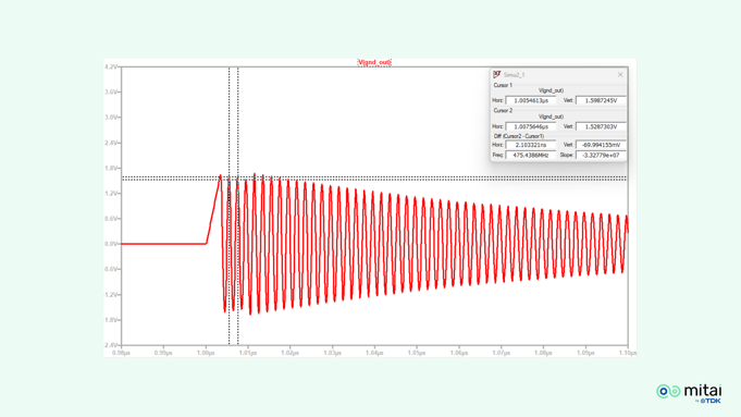
This looks much more like a physical signal, pseudo-sinusoidal with a period of about 2 ns (20 times the minimum simulation step). It should not come as a surprise, as the resonant frequency of the L-C circuit made of L_GND and Cd is: 1/(2 pi) / (1 nH x 100 pF)½ = 527 MHz - we are quite close.
Let’s pause and do two things:
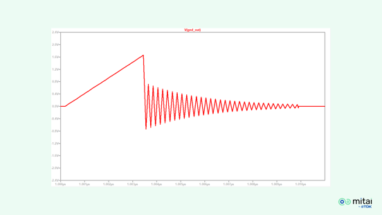
First, let’s find out the root cause of this behaviour and, to that end, let’s have a look at the current through L_GND:
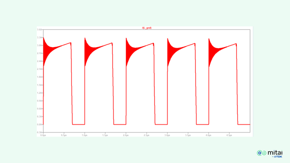
Zooming:
We see a very sharp rise of the current - in a few ns - from zero to the value of the output current. That’s quite logical: as soon as the switch starts conducting, diode D, which was freewheeling the output current, becomes reverse biased and switches off, so the output current, “pushed” by the main choke L, suddenly has no other path than to return to the negative side of Vi through the parasitic inductance L_GND.
"Now remember the basic law governing the voltage across an inductor":
V = L dI/dt… all is said.
The L in this formula is proportional to the area embraced by the loop traversed by the fast current variation, i.e. the loop made of the source capacitor Vi, the switch and the freewheeling diode D. The formula shows that the issue is proportional to this inductance, thus to this area, hence the first design rule:
Rule #1: minimise the area embraced by the loop made of the input capacitor, the switch, and the freewheeling diode.
Second, think about the meaning of this: even a minimal inductance causes a high frequency voltage with peak values around 1.5 V to appear across the ground connection between the input and the output of the buck converter - thus also between the GND pins of ICs and other components on the board - largely enough to cause nasty functional issues, especially on fast, low-level signals. It is also enough to generate external EMC issues between e.g. connectors and cables connected to the different parts of the circuit - and thus different grounds from a high frequency perspective.
The cure
What can we do about it? The answer is: not much, but…
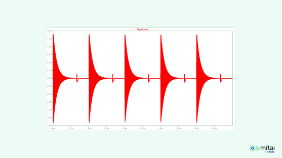
The first thing that springs to mind is to slow down the rate of rise of the current through the switch. We can do this, but it will come at the cost of increased switching losses in the switch - and there will still be some voltage ringing across L_GND, although with reduced amplitude.
A second idea would be to try and damp the oscillation, which can be achieved by adding a R-C circuit in parallel with the resonating capacitor, i.e. diode D in the present case.
The rule of thumb is simple: the added capacitor must be significantly larger than the resonating one, say five times, and the resistor can be approximated as ½ (L/C)½, thus is this case: Cam = 500 pF and Ram = 1.6 Ohm.
In practice, the value of the parasitic is of course not known precisely, but they can be determined experimentally and the values of Cam and Ram can then be calculated as explained above.
This will not come completely for free however, as, on top of the additional components themselves, the energy exchanged with the additional at every switching cycle of the transistor will be dissipated in the amortizing resistor; in this case: P = Cam x Vi² x f = 500 pF x 25 V² x 1MHz = 12.5 mW - generally acceptable for a 10 W converter as it degrades its efficiency by around 0.1 %.
Let’s try:
As we can see, the damping has done its job, so it was a good idea… but the initial voltage spike remains stubbornly in place and will still potentially perturbate the world around the converter.
There is actually a very simple and obvious solution to eliminate this effect without any additional component; let’s consider this slightly modified circuit:
We have not changed anything to the PCB netlist, as the parasitic inductor L_GND, being parasitic, is not part of it, but now there is obviously no voltage spike anymore between the negative polarity of the input “capacitor” Vi and that of the output “capacitor” Vo.
This remains true even if we add a parasitic inductor L_GND2 in this path:
There is still some voltage between the two nodes, but we are now in the mV range so this is much less likely to wreak havoc in the rest of the board.
We can thus derive our second design rule:
Rule #2; connect the negative of the output capacitor directly to the negative of the input capacitor; route separately the anode of the freewheeling diode to the negative of the input capacitor; avoid absolutely any common part between these two paths.
4. A multilayer PCB is also a current transformer
Now imagine that, according to rule #2, we have routed that critical track on, say, the top PCB layer. Following good practice, we’ll naturally use one of the inner layers, say, the second, as a continuous ground plane and connect the GND pins of all ICs and other devices to it.
Do you know planar transformers They use PCB tracks as windings, one layer holding for instance the primary and another the secondary winding. Like any transformer, their functional principle is current cancellation: when current is flowing in one winding, another current will flow in the opposite direction in the other coupled winding to very much cancel the magnetic field created by the first.
The windings of a transformer usually have multiple turns, but the same principle applies to windings with single turns.
And that’s exactly what we have done with our critical loop on the top layer and a ground plane on the second; the latter is just a transformer secondary, simply short-circuited.
Back to our model, this effect can easily be simulated by introducing a coupling factor between L_GND and L_GND2:
For the connoisseur, a coupling factor of 0.95 corresponds to a leakage inductance of about 10% - thus not an excessively tight coupling.
Let’s launch the simulation and check again the voltage between the two “ground” nodes:
Well, it looks as if we are back to square one…
Having a ground plane under the critical loop is actually a good idea, because it greatly helps to avoid spatial expansion of both the moderate AC electrical field caused by the swinging voltage on the “ac” node, and, more importantly, of the magnetic field caused by the fast current variation; it comes however at the cost having approximately the same current variation circulating through the ground plane.
Same cause, same cure:
Rule #3: Create a ground plane under the critical loop made of the input capacitor, the switch and the freewheeling diode BUT make an “island” of this part of the ground plane, connected to the rest of the ground plane only on one point, preferably at the negative connection of the input capacitor.
This means also that the negative end of the output capacitor must be connected to the “general” ground plane and not to this “island”. By doing so, we can revert to our previous model without coupling between the parasitic inductances.
Note also that the shielding effect of the ground plane is not perfect, partly because it is not a perfect short circuit at high frequencies because of the skin effect that reduces the effective copper thickness (6.5 µm at 100 MHz, 2 µm at 1 GHz) and thus increases its resistance. It is thus good practice to avoid running sensitive signal tracks on other layers beneath the critical loop.
5. An inductor is also a capacitor
No component is ideal, and the filtering inductor L is no exception. It is generally a wound component, where the proximity of multiple wires create a parasitic parallel capacitance whose value will vary with the geometry and the manufacturing process.
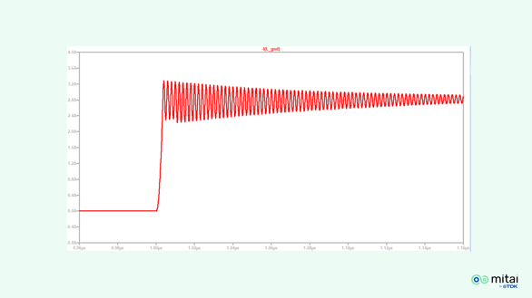
Let’s assume a value of 50 pF and look at what happens:
This time we get damped oscillations around 700 MHz on both switch ON and OFF events, with an amplitude an order of magnitude smaller than the one seen previously, but still large enough to create issues.
Where does it come from? Well, it(s more obvious this time: the voltage on node “ac” is basically a square wave, and we have a L-C circuit made of the main inductor parasitic capacitance C_L that we just introduced and the small inductor L_GND2. Let’s check its resonant frequency:
1/(2pi)/(LC)½ = 1/(2pi)/(10-9 x 50x10-12) = 745 MHz - again, close enough.
How can we improve?
A first guideline is to be careful when selecting the main inductor L and opt for a component with an as low as possible capacitance. This will certainly help, but some capacitance will inevitably remain.
A more radical solution is to make L_GND2 as low as possible, and it’s easy to do: just move the output capacitor against the input capacitor, interconnecting their negative terminals together as tightly as possible:
By doing this, we have moved the voltage oscillation on the other side of L_GND2, and it does not appear anymore between the GND on the input side and the GND on the output side, as they are one and the same node as far as can be achieved.
Hence:
Rule #4: Move the input and the output capacitors as close to each other as possible; connect their negative terminals together as tightly as possible.
Conclusion
This article went through the design considerations for Power Converters. Considering the real aspects of a circuit when designing power is key for good performance as well as for EMC compliance.