
PCB designs
About Author:
Reto B. Keller studied electrical engineering at Fachhochschule OST in Rapperswil SG, Switzerland. He works as Principal Electronics Development Engineer at Roche Diagnostics International Ltd., Rotkreuz Switzerland. He is a member of the IEC TC65 and is actively involved in developing EMC standards. As president of the Academy of EMC, and author of the open-access book "Design for Electromagnetic Compatibility - In a Nutshell", he publishes free knowledge about EMC for professional engineers.
Table of content:
1. Grounding Conductors
2. Return Current Through Ground Planes
3. PCB Grounding & EMC
4. Split Ground Planes vs Single Ground Planes
5. Common Impedance Coupling
Introduction
A mixed-signal design consists of analog and digital circuits on a single printed circuit board (PCB).
Every electronics design engineer is familiar with this question: Should we split the ground of our mixed-signal PCB into analog and digital ground? And if yes: How should we connect them? A good ground concept in a mixed-signal PCB design is essential to minimise noise, interference, power integrity, signal integrity, and electromagnetic compatibility (EMC) issues. This whitepaper explains grounding for mixed-signal PCB designs and show some pitfalls.
Grounding Conductors
In electronic circuits, ground conductors are the conductors through which the power supply return currents and the signal return currents flow. Ground planes on a PCB or grounding conductors in a system are often meant to be equipotential. However, this is not the case, as there is a voltage drop across the ground plane or along a ground conductor as soon as there is a current flowing because ground planes and ground conductors have an impedance Zg [Ω] that is greater than zero:
| 𝑍𝑔 | > 0 (1)
![Importance of Zg [Ω] Impedance in Return Current Signal Ground for Mixed Signals PCBs, Explained [1]](https://blog.mitai.ai/hs-fs/hubfs/Grounding%20Conductors-min.png?width=1900&height=993&name=Grounding%20Conductors-min.png)
Figure 1: Zg [Ω] is the impedance of the return current signal ground, which is not shown in any circuit schematic but present in every circuit [1].
It is practical to model the ground (plane or connector) as a series connection of a resistance Rg [Ω] and an inductance Lg [H]. This is a massive simplification. However, it is in many cases sufficient. The ground (plane or conductor) impedance can then be written as [1]:
𝑍𝑔=𝑅𝑔 + 𝑗𝜔𝐿𝑔 (2)
where Rg [Ω] is the ground resistance, Lg [H] the ground inductance and ω = 2𝜋f [rad/sec] is the angular frequency of a sinusoidal harmonic of the signal. Equation ( 2 ) shows us that the ground impedance is frequency dependent. For low-frequency signals, where the frequency f [Hz] is low (let’s say <100kHz), the dominant part in the term of Zg [Ω] is the resistance Rg [Ω]. However, once the frequency exceeds a certain limit (e.g. >1MHz), the reactance Xg = ωLg is going to become the dominant term in the equation.
Figure 2 shows the frequency dependent impedance Z(f) [Ω] of two ideal single round copper wires with length L=0.1m and diameters D=1mm and D=0.1mm.
The two graphs in Figure 2 visualize that it depends on the dimensions of interconnection if the reactance starts to be dominant at frequencies f<100kHz or at f>1MHz. Even if we consider the skin-effect of the wire, the reactance dominates at high frequency, because the reactance X=ωL increases with 20dB/decade and the resistance due to the skin-effect with 10dB/decade.
Please bear in mind that the graphs in Figure 2 (image below) represent a massive oversimplification and that things are much more complicated in real electronic designs. However, it gives an idea of the behavior of a (ground) conductor impedance for high frequency.
Ground conductors play an important role for the following design topics:
- Power and signal integrity
- Electromagnetic compatibility
Therefore, the next two sections will present a deeper understanding of why grounding is important for power/signal integrity and electromagnetic compatibility.
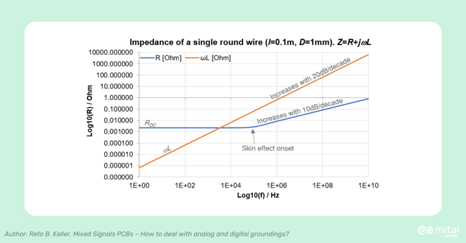
Figure 2: Impedance Z = R +jωL of a round wire with length L=0.1m
diameter D=1mm (Top Image) and D=0.1mm (Bottom Image).
Sources: R calculation equation 10.8 [1],
L calculation equation 6.2.1.1 [3].
-min.png?width=680&height=355&name=photos%20generated%20by%20AI%20(2)-min.png)
Return Current Through Ground Planes:
On a PCB, ground is the name for the return current conductor: signal currents of analog and digital circuits flow through the ground plane back to their sources.
As shown in Equation ( 2 ) and Figure 2, the ground impedance is dominated by the resistance Rg [Ω] for low frequencies and by the inductance Lg [H] for high frequencies. This means:
- At low frequencies (around f < 100 kHz), the signal return current path in the solid ground plane flows straight (see the return current in Figure 3 for low frequencies).
This is, because the resistance Rg [Ω] is the lowest for the direct connection form Via 1 to Via 2 in Figure 3
- At high frequencies (around f > 1MHz), the signal return current in the solid ground plane flows directly below the respective PCB trace (see the return current in Figure 3 for high frequencies).
This is because the high-frequency return currents take the path that minimizes the energy stored in the magnetic field, and that is when the area between the forward and return current is minimised.
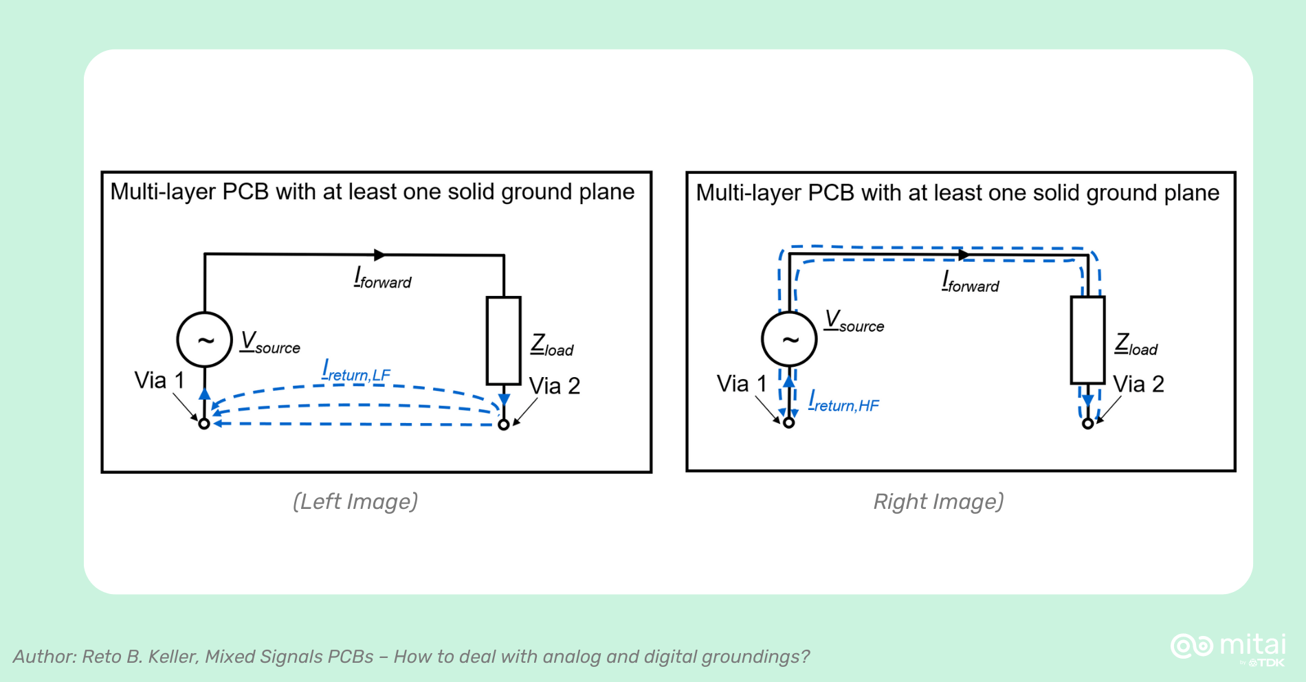
Figure 3: Signal return currents in a solid PCB ground plane.
Left Image: At low-frequencies (around f < 100 kHz).
Right Image: At high-frequencies (around f > 1MHz).
PCB Grounding And Power/Signal Integrity
Good grounding provides a low-impedance path for the return currents generated by the active components in a circuit. Here's why grounding is important and how improper grounding practices can worsen power and signal integrity:
-
Common Impedance Coupling (Ground Bounce):
Improper grounding can lead to ground bounce, which is the fluctuation in the ground reference voltage caused by switching signals. Ground bounce can result in voltage noise on power or signal lines, affecting the stability and functionality of the circuit. As soon as multiple power supplies or signals lines share a common ground plane or ground conductor, there is the possible chance that an intolerable noise voltage along the ground connection is introduced by alternating currents. -
Ground Loops:
Incorrect grounding practices can lead to ground loops, which are unintended current paths resulting from multiple ground connections. Ground loops introduce unintended currents that can cause noise, interference, and degrade signal quality.
PCB Grounding And Electromagnetic Compatibility
In addition to the power integrity relevant topics like common impedance coupling and ground loops, EMC design engineers must also take care of circuit loop areas A [m2] of high-speed signals (>1MHz).
The reason for this is that high-frequency signals potentially radiate at unacceptable high levels. Let’s assume an electrically small current loop (circumference < λ/4), so that the current distribution (magnitude, phase) is constant along the current loop and a measurement point of the E-field [V/m] in the far-field. The maximum root mean square (RMS) value of the electric field EDM,max [V/m] caused by a differential-mode current IDM [A] can be approximated as [2]:
[Equation] ( 3 )
Where IDM [A] is the RMS value differential current through the small current loop, f [Hz] is the frequency of the sinusoidal current signal, A [m2] is the area of the current loop, and d [m] is the distance of the center of the current loop to where the EDM,max [V/m] is measured.
![A small current loop (small with respect to the wavelength λ [m] of the signal) as an unintended antenna.](https://blog.mitai.ai/hs-fs/hubfs/photos%20generated%20by%20AI%20(3)-min.png?width=1900&height=993&name=photos%20generated%20by%20AI%20(3)-min.png) Figure 4: A small current loop (small with respect to the wavelength λ [m] of the signal) as an unintended antenna.
Figure 4: A small current loop (small with respect to the wavelength λ [m] of the signal) as an unintended antenna.
Equation ( 3 ) shows that the field strength is proportional to the signal frequency f [Hz] squared f2. Therefore, unintended radiated emission is not so much an issue for low-frequency signals (e.g., <100kHz), but for high-frequency signals (e.g., >1MHz).
Split Ground Planes vs. Single Ground Plane?
In a mixed-signal PCB design with analog circuits and digital circuits, there is often the discussion within the design teams if the ground should be split into analog ground AGND and digital ground DGND, or if there should be single solid ground. From my own experience, a PCB design with split ground planes does not perform better – regarding unintended radiated emissions – than a PCB design with a single solid ground plane. In addition, a PCB with a split ground plane makes it much more difficult to route the analog and digital signals.
Dr. Todd Hubing – past president of the IEEE Electromagnetic Compatibility Society and an outstanding EMC expert – finds clear words [4]: “Don’t gap your ground plane, there's never really a good reason to do that.” The following section explains why this is the case.
One problem with split ground planes is that they can lead to high radiated emissions in case signals are routed over the gap between the groud planes. This is especially true if the signal is a high-frequency signal, like a serial peripheral inerface (SPI) clock. When a signal is routed over a ground plane gap and the return current flows through the common connection point of the grounds, a large current loop may be the result (see Figure 5). From Equation ( 3 ), we know that the radiated emission is approximately proportinal to the current loop area A [m2] and proportional to the frequency f [Hz] squared f2.
A solution to this problem would be, that the signal is routed over the connection of the common ground planes (where AGND and GND are connected together).
%20and%20its%20return%20current%20(dashed%20line%20arrow)-min.png?width=1900&height=993&name=Forward%20signal%20(solid%20line%20arrow)%20and%20its%20return%20current%20(dashed%20line%20arrow)-min.png) Figure 5: Forward signal (solid line arrow) and its return current (dashed line arrow).
Figure 5: Forward signal (solid line arrow) and its return current (dashed line arrow).
However, as today's PCB designs are getting incredible dense and routing of signals is getting more complex. Therefore, it may be not practical to route all high-speed signals over the ground connection point of AGND and GND.
This is one of the reasons why it is best practice to go with one single solid GND.
Another reason, why splitting GND planes is not a good idea is the question: Where should the analog ground AGND and the digital ground GND be connected? Should it be connected at the analog-to-digital converter ADC? Or at the power supply? What if there are multiple ADCs and power supplies on a board: should AGND and GND be connected at every ADC or power supply separately or only once? If only once, at which ADC? Or should you implement different AGNDs, for every ADC converter, a separate AGND? These are all questions that arise, once you decide to split the ground planes. These questions are not easy to answer and there is no one-answer-fits-it-all because every design is different and what works in one case, may not work for the next design.
And then there is another fact when splitting the ground planes: stray capacitance coupling between the split planes. Even if you decide to split the planes, there is always a coupling between the planes, and high-frequency signals can be coupled from one plane to the other. This means that even if you split the planes, they are not 100% separated from each other. So why make the effort and split them if they are separate 100%?
Common Impedance Coupling
Figure 6 shows the principle of common impedance coupling. Common impedance coupling can lead to high noise in sensitive analog circuits (ground bounce), where a couple of millivolts are already a not acceptable high noise level.
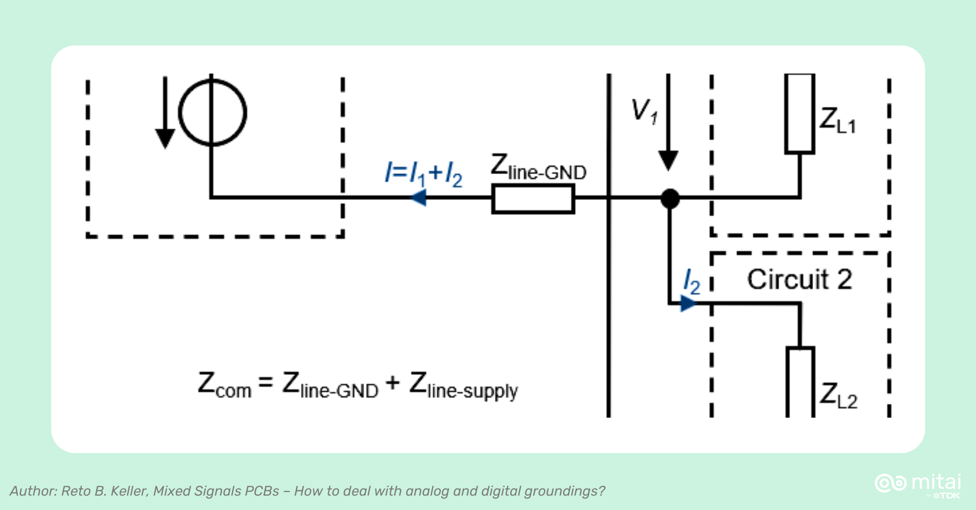 Figure 6: Common impedance coupling.
Figure 7 shows an example of a common impedance coupling with a high-power circuit and a sensitive analog circuit.
The current from the high-power circuit Ihp [A] introduces a noise voltage Vn [V] in the analog circuit:
𝑉𝑛 =𝑍𝑐𝑜𝑚 ∙ 𝐼ℎ𝑝 ( 4 )
where Zcom [Ω] is the common impedance of the sensitive analog circuit and the high-power circuit.
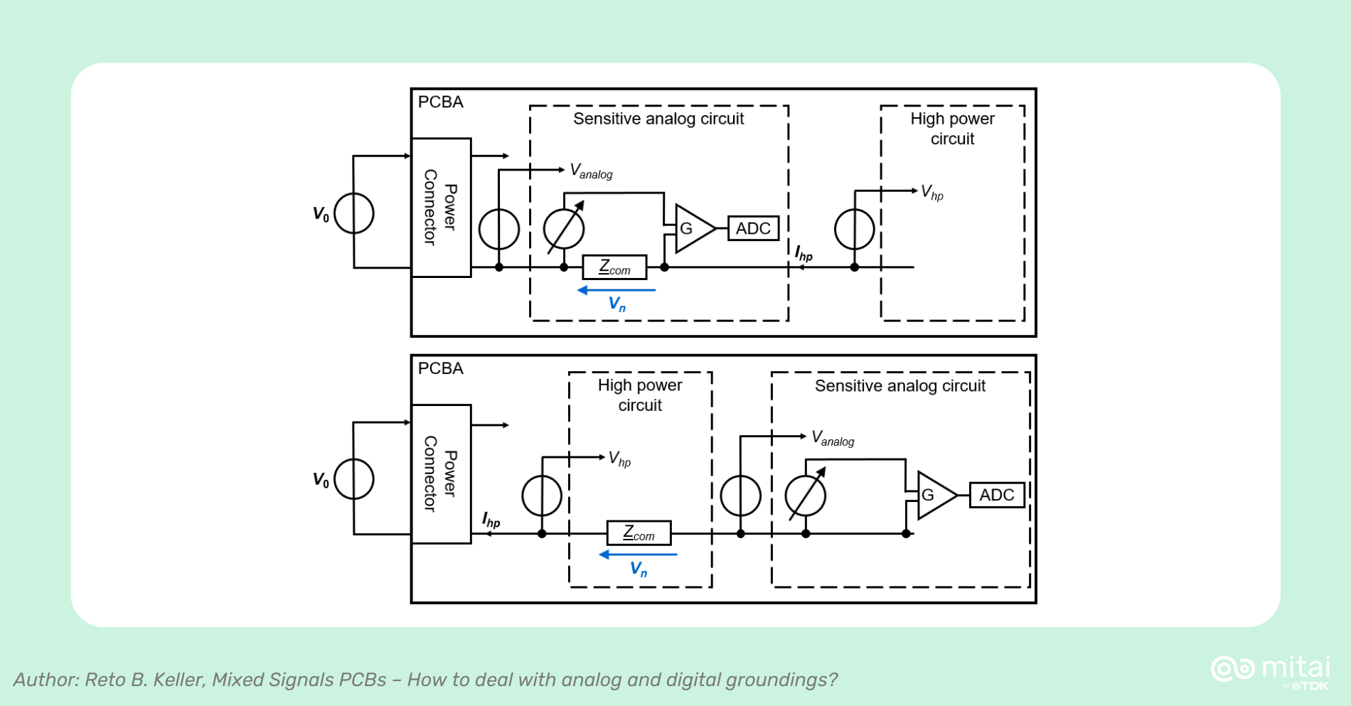
Figure 7: Common impedance coupling and how to minimize it.
Top: high noise levels in analog circuit. Bottom: Lower noise in analog circuit.
One way to minimize the noise voltage Vn [V] is to minimize the common impedance Zcom [Ω] by not placing the sensitive analog circuit between the power supply and the high-power circuit. Instead, the sensitive analog circuit is placed in a way, that the noise current does not affect the analog circuit minimally (see Figure 7).
Conclusion
It is best practice not to split or gap the ground of a mixed-signal PCB design into an analog and a digital ground plane. Splitting ground planes increase the complexity of the PCB design and could lead to high radiated emissions. Instead, go with a single solid ground plane and take care of the placing of the circuits, so that common impedance coupling is minimised.

Sources:
[1] Reto B. Keller. Design for Electromagnetic Compatibility - In a Nutshell. Theory and Practice. Springer, 2023.
[2] Clayton R. Paul. Introduction to electromagnetic compatibility. 2nd edition. JohnWiley & Sons Inc., 2008.
[3] Brian C. Wadell. Transmission line design handbook. Artech House Inc., 1991.
[4] Four Commonly Held Myths of EMC Design. YouTube channel of Altium. Interview with Dr. Todd Hubing. https://www.youtube.com/watch?v=TUS21J5RPE0&t=1313s [24. June 2023]